Pulse Check: How Intel is Scaling to Meet the Decade’s Opportunities

Eighteen months ago, Intel announced it would address the world’s rapidly growing computing continuum by investing in variations on the Intel Architecture (IA). It was met with a ho-hum. Now, many product families are beginning to emerge from the development labs and head towards production. All with IA DNA, these chip families are designed to be highly competitive in literally dozens of new businesses for Intel, produced in high volumes, and delivering genuine value to customers and end users.

Intel is the only company with an architecture, cash flow, fabs, and R&D capable of scaling its computing engines up and down to meet the decade’s big market opportunities. What is Intel doing and how can they pull this off?

The 2010’s Computing Continuum
Today’s computing is a continuum that ranges from smartphones to mission-critical datacenter machines, and from desktops to automobiles.  These devices represent a total addressable market (TAM) approaching a billion processors a year, and will explode to more than two billion by the end of the decade.  Of that, traditional desktop microprocessors are about 175 million chips this year, and notebooks, 225 million.

For more than four decades, solving all the world’s computing opportunities required multiple computer architectures, operating systems, and applications. That is hardly efficient for the world’s economy, but putting an IBM mainframe into a cell phone wasn’t practical. So we made due with multiple architectures and inefficiencies.

In the 1990’s, I advised early adopters NCR and Sequent in their plans for Intel 486-based servers. Those were desktop PC chips harnessed into datacenter server roles. Over twenty years, Intel learned from its customers to create and improve the Xeon server family of chips, and has achieved a dominant role in datacenter servers.

Now, Intel Corporation is methodically using its world-class silicon design and fabrication capabilities to scale its industry-standard processors down to fit smartphones and embedded applications, and up into high-performance computing applications, as two examples. Scaling in other directions is still in the labs and under wraps.

The Intel Architecture (IA) Continuum
IA is Intel’s architecture and an instruction set that is common (with feature differentiation) in the Atom, Core, and Xeon microprocessors already used in the consumer electronics, desktop and notebook, and server markets, respectively.  These microprocessors are able to run a common stack of software such as Java, Linux or Microsoft Windows.  IA also represents the hardware foundation for hundreds of billions of dollars in software application investments by enterprise and software application package developers that remain valuable assets as long as hardware platforms can run it — and backwards compatibility in IA has protected those software investments.

To meet the widely varying requirements of this decade’s computing continuum, Intel is using the DNA of IA to create application-specific variants of its microprocessors.  Think of this as silicon gene-splicing.  Each variant has its own micro-architecture that is suited for its class of computing requirements (e.g., Sandy Bridge for 2011 desktops and notebooks). These genetically-related processors will extend Intel into new markets, and include instruction-set compatible microprocessors:

  • Embedded processors and electronics known as “systems on a chip” (SOCs) with an Atom core and customized circuitry for controlling machines, display signage, automobiles, and industrial products;
  • Atom, the general-purpose computer heart of consumer electronics mobile devices, tablets, and soon smartphones;
  • Core i3, i5, and i7 processors for business and consumer desktops and notebooks, with increasing numbers of variants for form-factor, low power, and geography;
  • Xeon processors for workstations and servers, with multi-processors capable advances well into the mainframe-class, mission-critical computing segment;
  • Xeon datacenter infrastructure processor variants (e.g., storage systems, and with communications management a logical follow-on);

A Pause to Bring You Up To Date
Please do not be miffed: all of the above was published in February, 2011, more than two years ago. We included it here because it sets the stage for reviewing where Intel stands in delivering on its long-term strategy and plans of the IA computing continuum, and to remind readers that Intel’s strategy is hiding in plain sight for going on five years.

In that piece two years ago, we concluded that IA fits the market requirements of the vast majority of the decade’s computing work requirements, and that Intel is singularly capable of creating the products to fill the expanding needs of the computing market (e.g., many core).

With the launch of the 4th Generation Core 22nm microprocessors (code-name Haswell) this week and the announcement of the code-name Baytrail 22nm Atom systems on a chip (SoCs), it’s an appropriate time to take the pulse on Intel’s long-term stated direction and the products that map to the strategy.

Systems on a Chip (SoCs)
The Haswell/Baytrail launch would be a lot less impressive if Intel had not mastered the SoC.

The benefits of an SoC compared to the traditional multi-chip approach Intel has used up until now are: fewer components, less board space, greater integration, lower power consumption, lower production and assembly costs, and better performance. Phew! Intel could not build a competitive smartphone until it could put all of the logic for a computer onto one chip.

This week’s announcements include SoCs for low-voltage notebooks, tablets, and smartphones. The data center Atom SoCs, code-name Avoton, are expected later this year.

For the first time, Intel’s mainstream PC, data center, and mobile businesses include highly competitive SoCs.

SoCs are all about integration. The announcement last month at Intel’s annual investor meeting that “integration to innovation” was an additional strategy vector for the company hints at using many more variations of SoCs to meet Intel’s market opportunities with highly targeted SoC-based variants of Atom, Core, and Xeon.

Baytrail, The Forthcoming Atom Hero
With the SoCs for Baytrail in tablets and Merrifield in smartphones, Intel can for the first time seriously compete for mobile marketshare against ARM competitors on performance-per-watt and performance. These devices are likely to run the Windows 8, Android, and Chrome operating systems. They will be sold to carriers globally. There will be variants for local markets (i.e., China and Africa).

The smartphone and tablet markets combined exceed the PC market. By delivering competitive chips that run thousands of legacy apps, Intel has finally caught up on the technology front of the mobile business.

Along with almost the entire IT industry, Intel missed the opportunity that became the Apple iPhone. Early Atom processors were not SoCs, had poor battery life, and were relatively expensive. That’s a deep hole to climb out of. But Intel has done just that. There are a lot fewer naysayers than two years ago. The pendulum is now swinging Intel’s way on Atom. 2014 will be the year Intel starts garnering serious market share in mobile devices.

4th Generation Core for Mainstream Notebooks and PCs
Haswell is a new architecture implemented in new SoCs for long-battery-life notebooks, and with traditional chipsets for mainstream notebooks and desktops. The architecture moves the bar markedly higher in graphics performance, power management, and floating point (e.g., scientific) computations.

We are rethinking our computing model as a result of Haswell notebooks and PCs. Unless you are an intense gamer or workstation-class content producer, we think a notebook-technology device is the best solution.

Compared to four-year old notebooks in Intel’s own tests, Haswell era notebooks are: half the weight, half the height, get work done 1.8x faster, convert videos 23x faster, play popular games 26x faster, wake up and go in a few seconds, and with 3x battery life for HD movie playing. Why be tethered to a desktop?

Black, breadbox-size desktops are giving way to all-in-one (AIO) designs like the Apple iMac used to write this blog. That iMac has been running for two years at 100% CPU utilization with no problems. (It does medical research in the background folding proteins). New PC designs use notebook-like components to fit behind the screen. You’ll see AIOs this fall that lie flat as large tablets or go vertical with a rear kick-stand. With touch screen, wireless Internet and Bluetooth peripherals, these new AIOs are easily transportable around the house. That’s the way we see the mainstream desktop PC evolving.

And PCs need to evolve quickly. Sales are down almost 10% this year. One reason is global macro-economic conditions. But everybody knows the PC replacement cycle has slowed to a crawl. Intel’s challenge is to spark the PC replacement cycle. Haswell PCs and notebooks, as noted above, deliver a far superior experience to users than they are putting up with in their old, obsolescent devices.

Xeon processors for workstations, servers, storage, and communications
The data center is a very successful story for Intel. The company has steadily gained workloads from traditional (largely legacy Unix) systems; grown share in the big-ticket Top 500 high-performance computing segment; evolved with mega-datacenter customers such as Amazon, Facebook, and Google; and extended Xeon into storage and communications processors inside the datacenter.

The Haswell architecture includes two additions of great benefit to data-center computing. New floating point architecture and instructions should improve scientific and technical computing throughput by up to 60%, a huge gain over the installed server base. Second, transactional memory is a technology that makes it easier for programmers to deliver fine-grain parallelism, and hence to take advantage of multi-cores with multi-threaded programs, including making operating systems and systems software like databases run more efficiently.

In the past year, the company met one data-center threat in GPU-based computing with PHI, a server add-in card that contains dozens of IA cores that run a version of Linux to enable massively parallel processing. PHI competes with GPU-based challengers from AMD and nVidia.

Another challenge, micro-servers, is more a vision than a market today. Nevertheless, Intel created the code-name Avoton Atom SoC for delivery later this year. Avoton will compete against emerging AMD- and ARM-based micro-server designs.

Challenges
1. The most difficult technology challenge that Intel faces this decade remains software, not hardware.  Internally, the growing list of must-deliver software drivers for hardware such as processor-integrated graphics means that the rigid two-year, tick-tock hardware model must also accommodate software delivery schedules.

Externally, Intel’s full-fray assault on the mobile market requires exquisite tact in dealing with the complex relationships with key software/platform merchants: Apple (iOS), Google (Android), and Microsoft (Windows), who are tough competitors.

In the consumer space such as smartphones, Intel’s ability to deliver applications and a winning user experience are limited by the company’s OEM distribution model. More emphasis needs to be placed on the end-user application ecosystem, both quality and quantity. We’re thinking more reference platform than reference hardware.

2. By the end of the decade, silicon fabrication will be under 10 nm, and it is a lot less clear how Moore’s Law will perform in the 2020’s. Nevertheless, we are optimistic about the next 10-12 years.

3. The company missed the coming iPhone and lost out on a lot of market potential. That can’t happen again. The company last month set up an new emerging devices division charged with finding the next best thing around the same time others do.

4. In the past, we’ve believed that mobile devices — tablets and smartphones — were additive to PCs and notebooks, not substitutional. The new generation of Haswell and Baytrail mobile devices, especially when running Microsoft Windows, offer the best of the portable/consumption world together with the performance and application software (i.e., Microsoft Office) to produce content and data. Can Intel optimize the market around this pivot point?

Observations and Conclusions
Our summary observations have not changed in two years, and are reinforced by the Haswell/Baytrail SoCs that are this week’s proof point:

  • Intel is taking its proven IA platforms and modifying them to scale competitively as existing markets evolve and as new markets such as smartphones emerge.
  • IA scales from handhelds to mission-critical enterprise applications, all able to benefit from a common set of software development tools and protecting the vast majority of the world’s software investments.  Moreover, IA and Intel itself are evolving to specifically meet the needs of a spectrum of computing made personal, the idea that a person will have multiple computing devices that match the time, place and needs of the user.
  • Intel is the only company with an architecture, cash flow, fabs, and R&D capable of scaling its computing engines up and down to meet the decade’s big market opportunities.

Looking forward, Intel has fewer and less critical technology challenges than at any point since the iPhone launch in 2007. Instead, the company’s largely engineering-oriented talent must help the world through a complex market-development challenge as we all sort out what devices are best suited for what tasks. We’ve only scratched the surface of convertible tablet/notebook designs. How can Intel help consumers decide what they want and need so the industry can make them profitably? How fast can Intel help the market to make up its mind? Perhaps the “integration to innovation” initiative needs a marketing component.

If the three-year evolving Ultrabook campaign is an example of how Intel can change consumer tastes, then we think industry progress will be slower than optimal. A “win the hearts and minds” campaign is needed, learning from the lessons of the Ultrabook evolution. It will take skillsets in influencing and moving markets in ways Intel will need more of as personal computing changes over the next decade, for example, as perceptual computing morphs the user interface.

Absent a macro-economic melt-down, Intel is highly likely to enjoy the fruits of five years of investments over the coming two-year life of the Haswell architecture. And there’s no pressing need today to focus beyond 2015.

Biography

Peter S. Kastner is an industry analyst with over forty-five years experience in application development, datacenter operations, computer industry marketing, PCs, and market research.  He was a co-founder of industry-watcher Aberdeen Group in 1989.  His firm, Scott-Page LLC, consults with technology companies and technology users.

Twitter: @peterskastner
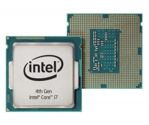
Haswell Core i7 desktop microprocessor

Haswell Core i7 desktop microprocessor


On the Impact of Paul Otellini’s CEO Years at Intel

Intel’s CEO Paul Otellini is retiring this week. His 40-year career at Intel now ending, it’s a timely opportunity to look at his impact on Intel.

Source: New York Times

Source: New York Times

Intel As Otellini Took Over

In September 2004 when it was announced that Paul Otellini would take over as CEO, Intel was #46 on the Fortune 100 list, and had ramped production to 1 million Pentium 4′s a week (today over a million processors a day). The year ended with revenues of $34.2 billion. Otellini, who joined Intel with a new MBA in 1974, had 30 years of experience at Intel.

The immediate challenges the company faced fell into four areas: technology, growth, competition, and finance:

Technology: Intel processor architecture had pushed more transistors clocking faster, generating more heat. The solution was to use the benefits of Moore’s Law to put more cores on each chip and run them at controllable — and eventually much reduced — voltages.

Growth: The PC market was 80% desktops and 20% notebooks in 2004 with the North America and Europe markets already mature. Intel had chip-making plants (aka fabs) coming online that were scaled to a continuing 20%-plus volume growth rate. Intel needed new markets.

Competition: AMD was ascendant, and a growing menace.  As Otellini was taking over, a market research firm reported AMD had over 52% market share at U.S. retail, and Intel had fallen to #2. Clearly, Intel needed to win with better products.

Finance: Revenue in 2004 recovered to beat 2000, the Internet bubble peak. Margins were in the low 50% range — good but inadequate to fund both robust growth and high returns to shareholders.

Where Intel Evolved Under Paul Otellini

Addressing these challenges, Otellini changed the Intel culture, setting higher expectations, and moving in many new directions to take the company and the industry forward. Let’s look at major changes at Intel in the past eight years in the four areas: technology, growth, competition, and finance:

Technology

Design for Manufacturing: Intel’s process technology in 2004 was at 90nm. To reliably achieve a new process node and architecture every two years, Intel introduced the Tick-Tock model, where odd years deliver a new architecture and even years deliver a new, smaller process node. The engineering and manufacturing fab teams work together to design microprocessors that can be manufactured in high volume with few defects. Other key accomplishments include High-K Metal Gate transistors at 45nm, 32nm products, 3D tri-gate transistors at 22nm, and a 50% reduction in wafer production time.

Multi-core technology: The multi-core Intel PC was born in 2006 in the Core 2 Duo. Now, Intel uses Intel Architecture (IA) as a technology lever for computing across small and tiny (Atom), average (Core and Xeon), and massive (Phi) workloads. There is a deliberate continuum across computing needs, all supported by a common IA and an industry of IA-compatible software tools and applications.

Performance per Watt: Otellini led Intel’s transformational technology initiative to deliver 10X more power-efficient processors. Lower processor power requirements allow innovative form factors in tablets and notebooks and are a home run in the data center. The power-efficiency initiative comes to maturity with the launch of the fourth generation of Core processors, codename Haswell, later this quarter. Power efficiency is critical to growth in mobile, discussed below.

Growth

When Otellini took over, the company focused on the chips it made, leaving the rest of the PC business to its ecosystem partners. Recent unit growth in these mature markets comes from greater focus on a broader range of customer’s computing needs, and in bringing leading technology to market rapidly and consistently. In so doing, the company gained market share in all the PC and data center product categories.

The company shifted marketing emphasis from the mature North America and Europe to emerging geographies, notably the BRIC countries — Brazil, Russia, India, and China. That formula accounted for a significant fraction of revenue growth over the past five years.

Intel’s future growth requires developing new opportunities for microprocessors:

Mobile: The early Atom processors introduced in late 2008 were designed for low-cost netbooks and nettops, not phones and tablets. Mobile was a market where the company had to reorganize, dig in, and catch up. The energy-efficiency that benefits Haswell, the communications silicon from the 2010 Infineon acquisition, and the forthcoming 14nm process in 2014 will finally allow the company to stand toe-to-toe with competitors Qualcomm, nVidia, and Samsung using the Atom brand. Mobile is a huge growth opportunity.

Software: The company acquired Wind River Systems, a specialist in real-time software in 2009, and McAfee in 2010. These added to Intel’s own developer tools business. Software services business accelerates customer time to market with new, Intel-based products. The company stepped up efforts in consumer device software, optimizing the operating systems for Google (Android), Microsoft (Windows), and Samsung (Tizen). Why? Consumer devices sell best when an integrated hardware/software/ecosystem like Apple’s iPhone exists.

Intelligent Systems: Specialized Atom systems on a chip (SoCs) with Wind River software and Infineon mobile communications radios are increasingly being designed into medical devices, factory machines, automobiles, and new product categories such as digital signage. While the global “embedded systems” market lacks the pizzazz of mobile, it is well north of $20 billion in size.

Competition

AMD today is a considerably reduced competitive threat, and Intel has gained back #1 market share in PCs, notebooks, and data center.

Growth into the mobile markets is opening a new set of competitors which all use the ARM chip architecture. Intel’s first hero products for mobile arrive later this year, and the battle will be on.

Financial

Intel has delivered solid, improved financial results to stakeholders under Otellini. With ever more efficient fabs, the company has improved gross margins. Free cash flow supports a dividend above 4%, a $5B stock buyback program, and a multi-year capital expense program targeted at building industry-leading fabs.

The changes in financial results are summarized in the table below, showing the year before Otellini took over as CEO through the end of 2012.

GAAP 2004 2012 Change
Revenue 34.2B 53.3B 55.8%
Operating Income 10.1B 14.6B 44.6%
Net Income 7.5B 11B 46.7%
EPS $1.16 $2.13 83.6%

The Paul Otellini Legacy

There will be books written about Paul Otellini and his eight years at the helm of Intel. A leader should be measured by the institution he or she leaves behind. I conclude those books will describe Intel in 2013 as excelling in managed innovation, systematic growth, and shrewd risk-taking:

Managed Innovation: Intel and other tech companies always are innovative. But Intel manages innovation among the best, on a repeatable schedule and with very high quality. That’s uncommon and exceedingly difficult to do with consistency. For example, the Tick-Tock model is a business school case study: churning out ground-breaking transistor technology, processors, and high-quality leading-edge manufacturing at a predictable, steady pace of engineering to volume manufacturing. This repeatable process is Intel’s crown jewel, and is a national asset.

Systematic Growth: Under Otellini, Intel made multi-billion dollar investments in each of the mobile, software, and intelligent systems markets. Most of the payback growth will come in the future, and will be worth tens of billions in ROI.

The company looks at the Total Addressable Market (TAM) for digital processors, decides what segments are most profitable now and in the near future, and develops capacity and go-to-market plans to capture top-three market share. TAM models are very common in the tech industry. But Intel is the only company constantly looking at the entire global TAM for processors and related silicon. With an IA computing continuum of products in place, plans to achieve more growth in all segments are realistic.

Shrewd Risk-Taking: The company is investing $35 billion in capital expenses for new chip-making plants and equipment, creating manufacturing flexibility, foundry opportunities, and demonstrating a commitment to keep at the forefront of chip-making technology. By winning the battle for cheaper and faster transistors, Intel ensures itself a large share of a growing pie while keeping competitors playing catch-up.

History and not analysts will grade the legacy of Paul Otellini as CEO at Intel. I am comfortable in predicting he will be well regarded.

Follow me on Twitter @PeterSKastner

Silvermont: Atom Steps Into the Spotlight

Intel unveiled its Silvermont architecture for Atom 22nm and 14nm chips yesterday. The billboard numbers are 5x lower power consumption and 3x more performance than the current Atom chips, which use the Saltwell architecture at 32nm. The first chips based on the Silvermont architecture, codenamed Baytrail for tablets and Merrifield for smartphones, should start shipping by the end of 2013.

Highlight: Performance and Power Excellence vs. ARM

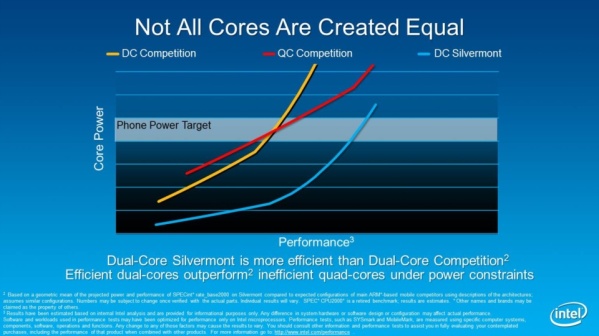
Intel projects the architecture will deliver significantly better performance, at lower power draw, than its ARM-based competition. Let’s get right to the fisticuffs.

Silvermont Performance/Power

Silvermont Performance/Power

In the chart above, Intel claims Silvermont-based Atom systems-on-a-chip (SoCs) will deliver more performance at lower battery draw in both dual-core (e.g., smartphone) and quad core (e.g., tablet) uses — at the time of product launch later this year. Moreover, Intel confidently predicts the dual-core Atom will beat quadcore ARM chips in performance and power usage. The gloves just came off.

Note though in the fine print that these are projected CPU performance based on architectural simulations. We’ll have to wait for the product launch for the real benchmark comparisons.

Is Intel just bluffing about wiping the floor with ARM on performance and power? We are strongly convinced that Intel is not bluffing; the launch videoconference was hosted at INTC.com, Intel’s investor relations portal where SEC-material announcements are made. Who in their right minds would want to bring the SEC and the class-action bar down on their heads with unwarranted and unsupportable benchmarketing claims?

Architecture Highlights

Our readers don’t want the full computer science firehouse on how the architecture works. A good review is AnandTech here. The important take-away points are:

  • Silvermont is a tour de force design that marries a custom version of Intel’s industry-leading, 22nm process with modern SoC design. It is optimized for low-power usage; new power-efficient design libraries were built and can be carried into other Intel architecture endeavors (i.e., Core).
  • Supports 2-8 cores in pairs. Each core has out-of-order execution (an Atom first), modern branch prediction, SIMD instructions, AES-NI security instructions, and Intel’s virtual technology (VT) for virtualization. Each pair of cores shares 1MB of level 2 cache. The design goal was low power consumption without sacrificing performance.
  • Like Atom’s big brother, Core, there is extensive on-chip digital power management including new power states. The SoC dynamically manages bursts of higher clock speeds, and looks  at first glance to be very sophisticated.
  • The overall dynamic power range is more efficient that ARM BIG:little approaches.

Where Will Silvermont Be Used?

The obvious places are in smartphones and tablets. Other than mentioning the market attractiveness of full Windows 8 on a tablet as well as the choice of Google’s Android — and maybe even a dual boot, let’s leave the smartphone and tablet war until another day when we compare real products. 

What we don’t hear today is talk about the likely growth for Silvermont-based Atom SoCs in markets other than phones and tablets. That’s a mistake because Intel surely has these markets in its sights:

  • Netbooks: Remember the 2008 low-cost Internet-consumption notebooks killed by ARM/Android by 2011? They’ll be back in spades. Lump Google Chromebooks in this category too.
  • Automotive: The abject failure of Ford’s My Ford Touch entertainment system using ARM and Microsoft Embedded Windows is the joke of the auto industry. Atom can play a role here as automobiles are today a processor-rich environment.
  • Retail Systems: Point-of-sale and checkout systems cry for low-power, small form-factor devices. Ditto ATMs.
  • Digital Signage: The market for personal ads on digital signage is just arriving. This will become a large market later in the decade.
  • Embedded Systems: Intel’s 2009 acquisition of Wind River Systems aimed to do more in real-time, embedded systems for healthcare, manufacturing, distributtion, automation,  and other activities. Silvermont-generation Atom chips are a big step forward for these markets.

Closing Thoughts

An architecture is not a testable or buyable product. Nevertheless, Silvermont looks to be the real deal for performance and power, and ought to be giving ARM licensees heartburn.

With the introduction of products based on the Silvermont architecture, Atom becomes a hero. Not a hero brand, but a hero family of chips that move out of the also-ran category to being in the spotlight as front-line performers in Intel’s many-chip continuum of computing strategy.

Silvermont is an important way-point in measuring Intel’s commitment and delivery of chips with: competitive power consumption, SoC maturity, and a new phone/tablet/embedded system workload target — without dropping the ball in the rest of the business. The proof of the architecture will be the Baytrail and Merrifield SoCs that start arriving by the holidays. And the Haswell announcement next month will clearly show Intel juggles multiple balls.

On balance, we are very pleased with the benchmark points that Intel promises to meet or exceed. That’s the proof of the pudding.

The 2013-2014 Computing Forest – Part 1: Processors

Ignoring the daily tech trees that fall in the woods, let’s explore the computer technology forest looking out a couple of years.
Those seeking daily comments should follow @peterskastner on Twitter.

Part 1: Processors

Architectures and Processes

Intel’s Haswell and Broadwell

We’ll see a new X86 architecture in the first half of 2013, code-name Haswell. The Haswell chips will use the 22 nm fabrication process introduced in third-generation Intel Core chips (aka Ivy Bridge). Haswell is important for extending electrical efficiency, improving performance per clock tick, and as the vehicle for Intel’s first system on a chip (SoC), which combines a dual-core processor, graphics, and IO in one unit.

Haswell is an architecture, and the benefits of the architecture carry over to the various usage models discussed in the next section.

I rate energy efficiency as the headline story for Haswell. Lightweight laptops like Ultrabooks (an Intel design) and Apple’s MacBook Air will sip the battery at around 8 watts, half of today’s 17 watts. This will dramatically improve the battery life of laptops but also smartphones and tablets, two markets that Intel has literally built $5 billion fabs to supply.

The on-chip graphics capabilities have improved by an order of magnitude in the past couple of years and get better of the next two. Like the main processor, the GPU benefits from improved electrical efficiency. In essence, on-board graphics are now “good enough” for the 80-th percentile of users. By 2015, the market for add-on graphics cards will start well above $100, reducing market size so much that the drivers switch; consumer GPUs lead high-performance computing (HPC) today. That’s swapping so that HPC is the demand that supplies off-shoot high-end consumer GPUs.

In delivering a variety of SoC processors in 2013, Intel learns valuable technology lessons for the smartphone, tablet, and mobile PC markets that will carry forward into the future. Adjacent markets, notably automotive and television, also require highly integrated SoCs.

Broadwell is the code-name for the 2014 process shrink of the Haswell architecture from 22nm to 14nm. I’d expect better electrical efficiency, graphics, and more mature SoCs. This is the technology sword Intel carries into the full fledged assault on the smartphone and tablet markets (more below).

AMD

AMD enters 2013 with plans for “Vishera” for the high-end desktop, “Richland”, an SoC  for low-end and mainstream users, and “Kabini”, a low-power SoC  for tablets.

The 2013 server plans are to deliver its third-generation of the current Opteron architecture, code name Steamroller. The company also plans to move from a 32nm SOI process to a 28nm bulk silicon process.

In 2014, AMD will be building Opteron processors based on a 64-bit ARM architecture, and may well be first to market. These chips will incorporate the IO fabric acquired with microserver-builder Seamicro. In addition, AMD is expected to place small ARM cores on its X86 processors in order to deliver a counter to Intel’s Trusted Execution Technology. AMD leads the pack in processor chimerism.

Intel’s better performing high-end chips have kept AMD largely outside looking in for the past two years. Worse, low-end markets such as netbooks have been eroded by the upward charge of ARM-based tablets and web laptops (i.e., Chromebook, Kindle, Nook).

ARM

ARM Holdings licenses processor and SoC designs that licensees can modify to meet particular uses. The company’s 32-bit chips started out as embedded industrial and consumer designs. However, the past five years has seen fast rising tides as ARM chip designs were chosen for Apple’s iPhone and iPad, Google’s Android phones and tablets, and a plethora of other consumer gadgets. Recent design wins includes Microsoft’s Surface RT. At this point, quad-core (plus one, with nVidia) 32-bit processors are commonplace. Where to go next?

The next step is a 64-bit design expected in 2014. This design will first be used by AMD, Calxeda, Marvell, and undisclosed other suppliers to deliver microservers. The idea behind microservers is to harness many (hundreds to start) of low-power/modest-performance processors costing tens of dollars each and running multiple instances of web application in parallel, such as Apache web servers. This approach aims to compete on price/performance, energy/performance, and density versus traditional big-iron servers (e.g., Intel Xeon).

In one sentence, the 2013-2014 computer industry dynamics will largely center on how well ARM users defend against Intel’s Atom SoCs in smartphones and tablets, and how well Intel defends its server market from ARM microserver encroachment. If the Microsoft Surface RT takes off, the ARM industry has a crack at the PC/laptop industry, but that’s not my prediction. Complicating the handicapping is fabrication process leadership, where Intel continues to excel over the next two years; smaller process nodes yield less expensive chips with voltage/performance advantages.

Stronger Ties Between Chip Use and Parts

The number of microprocessor models has skyrocketed off the charts the past few years, confusing everybody and costing chip makers a fortune in inventory management (e.g., write-downs). This really can’t keep up as every chip variation goes through an expensive set of usability and compatibility tests running up to millions of dollars per SKU (stock-keeping unit e.g., unique microprocessor model specs). That suggests we’ll see a much closer match between uses for specific microprocessor variations and the chips fabricated to meet the specific market and competitive needs of those uses. By 2015, I believe we’ll see a much more delineated set of chip uses and products:

Smartphones – the low-end of consumer processors. Phone features are reaching maturity: there are only so many pixels and videos one can fit on a 4″ (5″?) screen, and gaming performance is at the good-enough stage. Therefore, greater battery life and smarter use of the battery budget become front and center.

The reason for all the effort is a 400 million unit global smartphone market. For cost and size reasons, prowess in mating processors with radios and support functions into systems on a chip (SoCs) is paramount.

The horse to beat is ARM Holdings, whose architecture is used by the phone market leaders including Samsung, Apple, nVidia, and Qualcomm. The dark horse is Intel, which wants very much to grab, say, 5% of the smartphone market.

Reusing chips for multiple uses is becoming a clever way to glean profits in an otherwise commodity chip business. So I’ll raise a few eyebrows by predicting we’ll see smartphone chips used by the hundreds in microservers (see Part 2) inside the datacenter.

Tablets – 7″ to 10″ information consumption devices iconized by Apple’s iPad and iPad Mini. These devices need to do an excellent job on media, web browsing, and gaming at the levels of last year’s laptops. The processors and the entire SoCs need more capabilities than smartphones. Hence a usage category different from smartphones. Like smartphones, greater battery life and smarter use of the electrical budget are competitive differentiators.

Laptops, Mainstream Desktops, and All-in-One PCs – Mainstream PCs bifurcate differently over the next couple of years in different ways than the past. I’m taking my cue here from Intel’s widely leaked decision to make 2013-generation (i.e., Haswell) SoCs that solder permanently to the motherboard instead of being socketed. This is not a bad idea because almost no one upgrades a laptop processor, and only enthusiasts upgrade desktops during the typical 3-5 year useful PC life. Getting rid of sockets reduces costs, improves quality, and allows for thinner laptops.

The point is that there will be a new class of parts with the usual speed and thermal variations that are widely used to build quad-core laptops, mainstream consumer and enterprise desktops, and all-in-one PCs (which are basically laptops with big built-in monitors).

The processor energy-efficiency drive pays benefits in much lower laptop-class electrical consumption, allowing instant on and much longer battery life. Carrying extra batteries on airplanes becomes an archaic practice (not to mention a fire hazard). The battle is MacBook Air versus Ultrabooks. Low-voltage becomes its own usage sub-class.

Low End Desktops and Laptops – these are X86 PCs running Windows, not super-sized tablet chips. The market is low-cost PCs for developed markets and mainstream in emerging markets. Think $299 Pentium laptop sale at Wal-Mart. The processors for this market are soldered, dual-core, and SoC to reduce costs.

Servers, Workstations, and Enthusiasts – the high end of the computing food chain. These are socketed, high-performance devices used for business, scientific, and enthusiast applications where performance trumps other factors. That said, architecture improvements, energy efficiency, and process shrinks make each new generation of server-class processors more attractive. Intel is the market and technology leader in this computing usage class, and has little to fear from server-class competitors over the next two years.

There is already considerable overlap in server, workstation, and enthusiast processor capabilities. I see the low end Xeon 1200 moving to largely soldered models. The Xeon E5-2600 and Core i7 products gain more processor cores and better electrical efficiency over the Haswell generation.

Part 2: Form-Factors

Part 3: Application of Computing

Dell Inspiron 15z

Dell Inspiron 15z

Intel Pushes the Computing Continuum Down the 22nm Scale

Intel laid out its plans to aggressively use its new 22nm silicon process to dramatically lower processor voltages while actually improving performance over the next 30 months, the company told financial analysts at a conference on May 17 at headquarters in Santa Clara, California. What analysts heard was by far the clearest picture for a generation of silicon that I have ever heard the company articulate. The plan is especially attractive for the two-thirds of buyers who choose notebooks.

The plan is simple but audacious: use the industry-leading 22nm silicon process that Intel announced earlier this month to cut, for example, the median notebook power requirements to about 18 watts from the 35 watts on today’s 32nm Sandy Bridge process and architecture; then ramp volumes across the product line so that half the company’s volume entering 2014 uses the lower-power, better-performance silicon.

First, lowering power consumption as measured in watts — cut in half — without cutting performance means twice the battery life. For notebook users, that means a choice between a much thinner and lighter laptop — can you say “Apple MacBook Air for the masses at mass market prices?” — without losing battery life, or alternatively, twice the battery life. Intel is calling the next generation of thin-and-light notebooks “ultrabooks”, a trademark.

Second, these relative benefits will also accrue across the computing spectrum to desktops and servers, and especially enhancing Intel’s ability to deliver Systems on a Chip (SOCs) with Atom processors running at below a watt in tablets and smartphones. Lower electrical consumption is a high-priority in data centers and a growing priority and mandate in office desktops.

Why would Intel paint such a clear roadmap for the Ivy Bridge (2012) and Haswell (2013) generations of processors in a highly competitive market? In spite of record sales and profits, Intel’s stock is stuck in the low $20’s as some on Wall Street anticipate an Intel near-death experience from the late delivery of competitive smartphone and tablet chips. That won’t happen. The company wants investors to know that it’s not behind the eight-ball. Driven by rapidly growing emerging markets for traditional PCs and notebooks and a robust and continuing data center refresh cycle, the company claims it will grow at double-digit rates over the next three years without any revenue needed from smartphones and tablets.

But those Intel-based market-changing tablets and smartphones are coming, with highly competitive products in 2012 and after.  Across a global economy and time, I believe tablets and smartphones are an additive computing market opportunity. Intel’s SOC engine, the Atom processor line, gains from planned process improvements from today’s 45nm to 14nm in 2o14 across three nodes of silicon process in three years — about twice the rate of Core and Xeon microprocessors.

A second reason that Intel paints such a clear roadmap is the company’s total confidence in the recently announced 22nm process. The fact that Intel will produce all of its 2012 Ivy Bridge microprocessors using 100% 3D tri-gate 22nm transistors tells me the company is convinced it has the technology completely in hand. And the company upped the cap-ex ante this year, deliberately building more 22nm chip-making capacity to come online next year.

Is lower voltage and hence lower electrical consumption that big a deal? Yes, it certainly is. The original MacBook Air, the archetypical thin-and-light notebook launched in January 2008, uses a 17 watt Intel Core 2 microprocessor with dual cores at 1.4 GHz. This year, 32nm Sandy Bridge ultra-low voltage chips will clock 1.7 GHz with quad processors at 17 watts —  plus Turbo 2.0 temporary speed boosts up to 2.9 GHz. Ivy Bridge (22nm) in 2012 and the new Haswell micro-architecture in 2013 will improve that further.

The 2008 dual-core processor in the MacBook Air was a trade-off in notebook weight versus processor speed — the processor was OK but no speed demon. The quad core Sandy Bridge and subsequent generations are in the middle of notebook performance curves, now offering excellent computation capabilities while still sipping lightly from the battery. Mainstream notebooks will quickly migrate down to the 1.5-3.0 pound level, offer all day battery power, and a no-compromises user computing experience. They will be ultra-thin, ultra-responsive, and, with hardware and DNA from the McAfee acquisition, ultra-secure. As a road warrior, I look forward to taking permanently taking five pounds of carry weight off my shoulder.

The Atom processor will follow a similar but steeper power-to-performance curve as the heart of devices from the 0.1 watt to 10 watt range. As a betting technologist, the cards Intel dealt last week tell me Intel will have an easier job scaling power requirements down going forward than ARM processors will scaling performance up.

In fall 2009, the company said it was scaling from gadgets to mainframe-class serversacross the computing continuum with one Intel Architecture, and a common set of software, tools, and developer experience. Last week, the company said it was confidently using its new 22nm technology to push the computing continuum down the voltage curve, with benefits to all kinds and levels of computing. Having voluntarily laid its cards and reputation on the table, Intel is surely planning on under-promising and over-delivering. I would not bet against it.


Thoughts on Intel’s New 22nm 3D Transistors

Intel’s announcement yesterday announced the next generation of transistor process at 22 nm. New products based on the 22 nm transistors will begin arriving with the Ivy Bridge family in early 2012. What was not expected was that Intel would bet the fab on a radically new way of laying down transistors that puts the company a generation ahead of the silicon industry.

After briefings by Intel executives yesterday, my conclusions are that Intel has really ahead. I’ve sat through four previous generations of new transistor announcements, and it was the latest that got my serious attention.

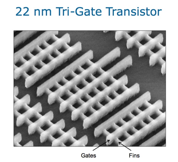
The science of what Intel has done is relatively easy to explain (see more depth here andhere): for fifty years, integrated circuits have been laid out like city street-maps in two dimensions, called “planar”. As the fabrication process has shrunk now to 22 nm, the shrinking physical area of each transistor creates huge problems in current leakage and gate current. Intel could have done another generation by shrinking its Sandy Bridge 32 nm transistors to 22 nm planar transistors, while picking up modest — 10%-20% performance was widely speculated — performance and power improvements. While Intel would be first to market with 22 nm, ten percent or so improvements is a ho-hum to the (jaded) computer industry. But Intel announced a switch to an industry-first three-dimensional transistor, fooling the market watchers.

3D transistors are laid on top of the usual circuit layout (see photo below). 3D transistor gates are wrapped around three sides of a vertical fin, hence the name tri-gate. Those three-sided contact points make the transistor much more efficient that planar transistors:

  • 3D transistors work with much less input current
  • allowing for a doubling of density, hence smaller chips
  • requiring about half as many power transistors.

The Benefits of Intel’s 22nm Transistors
Compared to today’s Sandy Bridge 32 nm transistors,  22nm 3D transistor microprocessors will perform as well at half the power. For mobile, your battery life doubles. This has enormous implications for mainstream thin-and-light Core family notebooks in 2012 followed by Atom-based tablets and smartphones. For desktops and servers, you’ll see a growing family of more power-efficient processors slotted to electricity-constrained environments.

At the same power levels as today’s Sandy Bridge 32 nm transistors, you’ll find Ivy Bridge performing about 37% faster — a lot more eye-opening than 10%-20% we anticipated.

The much improved power-performance ratio that we’ll see in Ivy Bridge with 22nm silicon gives Intel great leeway in creating enticing products. I expect:

  • Overclockers will push 6GHz while performance SKUs exceed 4.0GHz
  • An expanded Turbo range of 1-1.5GHz allowing for a performance boost at whim
  • Apple MacBook Air for the masses. Or at least the mainstream 1.5lb $600 Windows business laptop.
  • By 2013, the tablet and smartphone war with ARM will see pitched battles. Ultra-low voltage Intel microprocessors finally have close-enough battery life to compete head-to-head.
  • With a wider range of performance and power-sipping product opportunities, we’ll see more and different form factors.

Where 22nm 3D Transistors Place Intel
With 22nm planar transistors, Intel would lead the microprocessor industry. But the third-dimension transistors on top of a 22nm process likely put Intel two nodes ahead of the competition. Intel will lead in production-ready transistor technology for at least four years.

The fact that Intel will produce all of its 2012 Ivy Bridge microprocessors using 100% 3D tri-gate 22nm transistors tells me the company is convinced it has the technology completely in hand.

All in all,  22nm 3D transistors are truly revolutionary. By expanding the gate area with a 3D vertical fin, Intel is showing a higher-probability path to continuing Moore’s Law at 10nm and below in the 2015 timeframe. That assurance alone is worth tens of billions to the technology industry.

22nm tri-gate transistor
ricechex
General Mills Rice Chex